The Unified Extensible Firmware Interface, UEFI for short, serves as the brain of your system’s most fundamental operations. It’s the first code that runs when you power on your machine, guiding the boot process and bridging the gap between your hardware and operating system. Despite its critical role, this component remains a mystery for many — its complexity and low-level operation often deters even the most seasoned security researchers from exploring it, but what if you could take a peek behind the curtain? What if you can gain access to your device’s UEFI image, analyze its contents, and uncover what lies beneath? Imagine harnessing it into a killer implant feature-rich loader!
Dumping firmware isn’t just about curiosity; it’s a gateway to understanding and securing your system on a deeper level. Whether you’re a security researcher, a firmware enthusiast, or someone who loves to tinker with low-level components, dumping firmware opens up a world of possibilities!
In this blog post, I’ll walk you through the process of dumping UEFI firmware from a live system via software. We’ll explore various registers, consult the Intel Software Development Manual, and follow best practices to safely and effectively extract this image yourself, so you, too, can start diving into the heart of your system. Let’s get started.
Publicly available tools like CHIPSEC can obtain the UEFI image. It’s a powerful tool, no doubt, but when it comes to compromising the UEFI image of your my machine, simply loading it won’t cut it…hehehe
What’s Needed
This project will take place on an Intel 12th Generation i7-1270PE, which is based off of the 600 series chipset. The family platform controller hub for this CPU can be found here.
Realistically you can get by from referencing my data but you mayyyy run into a chipset using a particular offset differently. Would be ideal just to reference just in case 🙂
Weapons of choice:
- Visual Studio 2022 with the WDK installed for Windows 11 (preferably)
- A signed driver (feeling adventurous)
- Windows Kernel programming experience (This is not a how-to for kernel programming)
- Willingness to endure pain
This project will only apply for Intel based systems. If you have an AMD system, you will need to see how this would translate for AMD!
Acquiring the Firmware
Platform Controller Hub (PCH)
The Platform Controller Hub (PCH) is a critical component in modern computers, acting as a central hub for data transfers between the CPU, RAM, and peripherals. It manages essential I/O devices including USB ports, SATA controllers, and PCIe slots, while also supporting advanced features such as Rapid Storage Technology, Smart Sound Technology, Intel’s Management Engine, etc. The PCH’s extensive control over system components makes it an attractive target for vulnerability research, bootkit development, and achieving extreme persistence like your favorite Nation State actors.
Security researchers have demonstrated the PCH’s critical role in system security. For example, Satoshi’s SmmExploit showed how UEFI vulnerabilities can enable attackers to tamper with critical system components, successfully compromising an endpoint with Virtualization Based Security (VBS) and Hypervisor-enforced Code Integrity (HVCI) enabled…Wild!
While not directly PCH-related but demonstrating innovative persistence techniques, researchers have also explored persistence mechanisms leveraging PCIe-connected components, such as GPUs. Notable examples include Jellyfish, a Linux-based GPU rootkit leveraging OpenCL’s API to establish persistence within GPU memory, a component that can be reached via PCIe slots. Similarly, Smelly of Vx Underground developed a Proof-of-Concept GPU memory rootkit for Nvidia hardware, leveraging Nvidia’s API to manage logic and interactions over the PCIe bus.
These three examples highlight the PCH’s susceptibility to exploitation and its importance in maintaining system integrity.
The PCH is essential because it provides access to the UEFI image, which resides in flash memory connected via Serial Peripheral Interface (SPI). It features two SPI interfaces: SPI0, dedicated to managing flash memory operations, and SPI0 support for Trusted Platform Module (TPM) functionality. The SPI0 interface for flash is further divided into six distinct regions, as shown in Table 81: SPI0 Flash Regions:

Serial Peripheral Interface (SPI)
The PCH exposes registers and control bits within its PCI configuration space, enabling software to interact with the SPI controller. Accessing this address space involves calculating values for the bus, device, function, and offset, using a simple and straightforward algorithm as shown below:
DWORD GetPciValue(USHORT Bus, USHORT Device, USHORT Function, USHORT Offset)
{
    return 0x80000000 | Bus << 16 | Device << 11 | Function << 8 | Offset;
}
Think of this as plugging in the address of your Tinder date on a Friday night. You plug in the necessary values and voila! You know exactly where to meet your date. Well, same here. You plug in the bus, device, function, and offset (if applicable), and now you know where to read and write to! Hopefully, the SPI controller doesn’t ghost you — a technique I’m all too familiar about!
The resulting PCI value is typically used with x86 assembly IN and OUT instructions to perform low-level register access. For example:
mov eax, PCI_VALUE ; The value from GetPciValue
mov dx, 0xcf8      ; PCI_CONFIG_ADDRESS
out dx, eax        ; Write the calculated PCI address
mov dx, 0xcfc      ; PCI_DATA_PORT
in eax, dx         ; Read the data from the register
By plugging the address into these instructions, you can access the precise register you’re targeting. Just don’t swipe left on the bus, device, or function; otherwise, you’ll end up in the wrong neighborhood and an angry date!
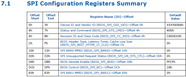
The SPI interface is a key component, as it controls access to the SPI flash memory where the UEFI image is stored. On Intel 600 and 700 series chipsets, the SPI controller is located at Bus 0, Device 31, Function 5. This address maps to the SPI Configuration Registers block, which includes all the registers and control bits necessary for interacting with the SPI controller, as shown below:

Some third-party vendors attempt to obscure the SPI interface by masking the Device ID and Vendor ID at offset 0x00000000 with -1. Nice try, but this “security measure” is more of a speed bump than a roadblock. You can still identify the SPI controller’s physical base address by querying the Base Address Register 0 (BAR0) at offset 0x00000010.
By reading BAR0 anyways, you effectively bypass this attempt at obfuscation, gaining access to the SPI interface. This underscores the classic phrase: security through obscurity. Am I right, or am I right??
The SPI BAR0 MMIO (Memory-Mapped I/O) is a structure that represents the region that describes the SPI memory-mapped registers. The SPI BAR0 MMIO is represented below:
union BIOS_SPI_BAR0
{
	struct
	{
		ULONG MemorySpace : 1;
		ULONG Type : 2;
		ULONG Prefetchable : 1;
		ULONG MemorySize : 8;
		ULONG MemoryBar : 20;
	};

	ULONG AsULong;
};
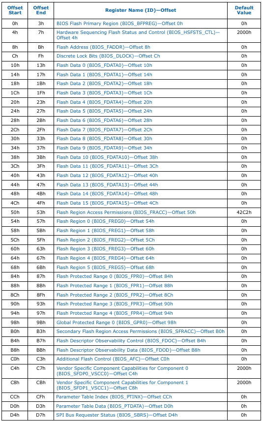
The SPI memory-mapped registers are shown below:

This region is essential for interacting with the SPI controller, as it holds all the necessary information to perform operations, including extracting the UEFI image.
Although this blog post focuses on UEFI, the SPI bus offers the opportunity to experiment with other peripherals. By exploring these devices, you can tamper modify analyze their firmware or memory spaces — opening a fascinating avenue for research and learning! 🙂
SPI Registers
BIOS Flash Primary Region
The BIOS Flash Primary Region member is a ULONG that represents the core memory segment of flash storage where the main firmware, including the UEFI image, resides. This region is critical because it contains essential system code and data required for the initial boot sequence, hardware initialization, and system management before the operating system fully loads.
The C++ representation of the BIOS Flash Primary Region register is shown below:
union BIOS_BFPREG
{
	struct
	{
		ULONG BiosFlashPrimaryRegionBase : 15;  // Base address of the primary region
		ULONG Reserved : 1;                     // Reserved
		ULONG BiosFlashPrimaryRegionLimit : 15; // Limit of the primary region
		ULONG Reserved2 : 1;                    // Reserved
	};

	ULONG AsULong;
};
This register provides the base address and limit of the BIOS flash primary region, defining its location and size within the SPI flash memory. The base address specifies where the primary region begins, while the limit determines its end. Together, these fields enable precise location and access to firmware components stored in this region.
Calculating the base address of the primary region and the size of the image relies on information from the SPI BAR0 MMIO, specifically the MemorySize and MemoryBar members. These members are hardwired to zero to indicate that the MemoryBar is aligned to a 4KB boundary, and the region spans 4KB of memory.
This information is important for operations like reading or modifying firmware, as it ensures precise targeting of the desired flash memory segment. Understanding and working with this register forms the foundation for tasks such as UEFI image extraction and comprehensive firmware analysis.
Hardware Sequencing Flash Status and Control
The Hardware Sequencing Flash Status and Control (HSFSTS) member is a ULONG that uses individual bits to represent various control and status flags. Below is the C++ representation for reference:
union BIOS_HSFSTS_CTL
{
	struct
	{
		ULONG FlashCycleDone : 1;
		ULONG FlashCycleError : 1;
		ULONG AccessErrorLog : 1;
		ULONG Reserved : 2;
		ULONG SpiCycleInProgress : 1;
		ULONG Reserved2 : 5;
		ULONG WriteStatusDisable : 1;
		ULONG PRR34_LOCKDN : 1;
		ULONG FDOPSS : 1;
		ULONG FDV : 1;
		ULONG FLOCKDN : 1;
		ULONG FGO : 1;
		ULONG FCYCLE : 4;
		ULONG WET : 1;
		ULONG Reserved3 : 2;
		ULONG FDBC : 6;
		ULONG Reserved4 : 1;
		ULONG FSMIE : 1;
	};

	ULONG AsULong;
};
The HSFSTS register serves as the main communication channel with the SPI controller, enabling control over all flash memory operations. Several members of the HSFSTS register provide real-time feedback on operation status. For instance, the FlashCycleDone member is set by the CPU when a flash cycle completes, making it a key indicator to monitor during operations. In cases of errors, the FlashCycleError and AccessErrorLog members are set, signaling issues such as attempting to access restricted memory regions without proper permissions.
Control over flash operations is managed primarily through the FCYCLE and FGO bits. While my focus for this blog post is extracting the UEFI image, which only requires read operations, the FCYCLE member can initiate several types of flash cycles, including:
- Read (for data extraction)
- Write (for data modifications)
- 4K Block Erase and 64K Sector Erase (for clearing specific memory regions)
- Read Serial Flash Discoverable Parameters (SFDP)
- Read JEDEC ID (for device identification)
- Write Status and Read Status (for status configuration)
- RPMC Op1 and RPMC Op2 (for RPMC operations)
To start a flash operation, the desired type is set in the FCYCLE member, and the FGO bit is set to begin the flash operation. Monitoring the status flags — FlashCycleDone, FlashCycleError, and AccessErrorLog — is important for effective error handling and troubleshooting.
After setting the type of flash operation in the FCYCLE member, the FGO bit is set to begin the flash operation. For example, after initiating a cycle, check FlashCycleDone to confirm successful completion. If FlashCycleError is set, review the permissions and command parameters, clear the error flag and retry. If AccessErrorLog is set, ensure the targeted memory region has the appropriate access level and adjust the address if necessary.
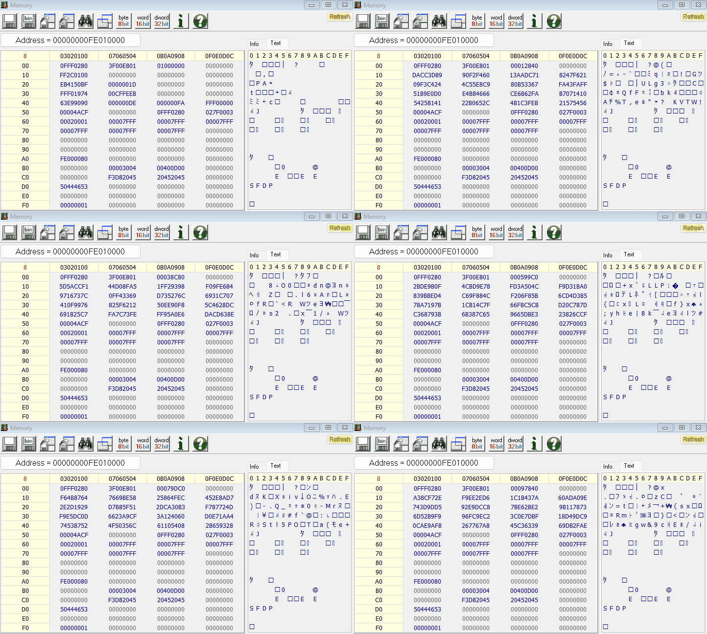
For reading data from flash memory, setting FCYCLE to Read enables the necessary flash operations. During the process, monitoring FlashCycleDone ensures that each segment completes as expected. Since each read cycle retrieves up to a maximum of 64 bytes, extracting the full UEFI image requires a sequential series of commands to cover the entire region. Watching these operations in real-time with tools like RWEverything, as the SPI controller iterates through the flash cycle commands, is very interesting to see! Who would have thought a simple ULONG could have so much influence?
The Flash address
The Flash Linear Address specifies the starting point for the SPI controller’s read operations. This address determines where the controller begins accessing data within the SPI flash memory. If the target region lacks the necessary access permissions, the I/O operation will fail, resulting in errors in FlashCycleError or AccessErrorLog.
When extracting UEFI images, the Flash Linear Address corresponds to the specific region being iterated through in the flash memory. Each flash region is defined by its base address and limit, as outlined in the SPI configuration. By calculating and setting the correct linear address, you can target the desired region and ensure accurate data retrieval during the extraction process.
Flash Data
The Flash Data array, consisting of 16 DWORDs, stores the data retrieved by the SPI controller during a read operation. Each read cycle retrieves up to 64 bytes of data, as determined by the size specified in the Flash Data Byte Count member of the HSFSTS register. Unlike a typical file download where data is transferred in a single continuous stream, retrieving flash data requires sequential commands. Each command directs the SPI controller to read the next chunk of data until the entire UEFI image is retrieved.
Watching the SPI controller process data 64 bytes at a time with tools like RWEverything is such a cool thing to watch — like watching someone fill a gallon of water using one cup at a time!
Error Registers
The error registers include three key status bits: Flash Cycle Done, Flash Cycle Error, and Access Error Log. These bits, the lower three bits of the HSFSTS register, are critical for monitoring the success of a flash operation.
- Flash Cycle Done: This bit indicates that the flash cycle has completed successfully. It should be checked after each operation to confirm proper execution.
- Flash Cycle Error: If set, this bit signals that an error occurred during the operation, such as invalid parameters or permission issues.
- Access Error Log: This bit logs access violations, which often occur when attempting to interact with restricted or protected regions of flash memory.
If any of these bits are set, it means something went wrong during the operation. Proper error handling involves diagnosing the issue, clearing the error flags, and retrying the operation with corrected parameters or permissions.
Pulling it all together
The goal of this project is to extract the UEFI image via SPI interface; however, the same method can be repurposed to interact with other peripherals on the bus, such as leveraging GPU memory as mentioned earlier. This process begins by resolving the SPI base address, which is calculated using the BAR0 register. According to Intel’s 700 series datasheet, the base address aligns to a 4KB boundary and is mapped into the process’ address space for further interaction:
DWORD dwSpiBaseAddress = bar0.MemoryBar << 12;
DWORD dwSpiSize = 1 << 12;
At this point, we have a pointer to the SPI Memory-Mapped structure, as previously discussed.
The next step involves calculating the size of the UEFI region. This is done by taking the value from the BiosFlashPrimaryRegionLimit member, aligning it to a 4KB boundary, and adding 1 to account for the entire region. The calculation is implemented below:
dwUefiRegionSize = pSpiFlashMemory->BiosFlashPrimaryRegion.BiosFlashPrimaryRegionLimit;
dwUefiRegionSize = ((dwUefiRegionSize << 12) | 0xfff) + 1;

pUefiRegionAsBytes = std::make_unique<BYTE[]>(dwUefiRegionSize);
Once the size is calculated, the program iterates through the six defined flash regions to validate their boundaries and extract data. Each region is checked to ensure the base address is not larger than the limit, as this would indicate an invalid region:
for (DWORD dwRegionIndex = 0; dwRegionIndex < ((sizeof(pSpiFlashMemory->FlashRegion) / sizeof(pSpiFlashMemory->FlashRegion[0])) << 1); dwRegionIndex++)
{
    UefiTypes::BIOS_FREG BiosFreg = pSpiFlashMemory->FlashRegion[dwRegionIndex];
    DWORD dwRegionBase = BiosFreg.RegionBase << 12;
    DWORD dwRegionLimit = ((BiosFreg.RegionLimit << 12) | 0xfff) + 1;

    if (dwRegionBase > dwRegionLimit)
    {
        continue;
    }
  --snipped--
For valid regions, the SPI controller begins reading data in 64-byte increments. The FlashCycleDone flag is monitored to ensure each cycle completes successfully, and the data is copied from the SPI flash memory into the allocated buffer:
  --snipped--
    pSpiFlashMemory->FlashAddress.FlashLinearAddress = dwRegionBase;

    do
    {
        pSpiFlashMemory->HardwareSequencingFlashStatusAndControl.FDBC = 64 - 1;
        pSpiFlashMemory->HardwareSequencingFlashStatusAndControl.FCYCLE = static_cast<DWORD>(UefiTypes::HSFSTS_CYCLE::Read);
        pSpiFlashMemory->HardwareSequencingFlashStatusAndControl.FGO = 1;

        while (!pSpiFlashMemory->HardwareSequencingFlashStatusAndControl.FlashCycleDone);

        if (!pSpiFlashMemory->HardwareSequencingFlashStatusAndControl.FlashCycleError &&
            !pSpiFlashMemory->HardwareSequencingFlashStatusAndControl.AccessErrorLog)
        {
            for (DWORD dwIndex = 0; dwIndex < sizeof(pSpiFlashMemory->FlashData) / sizeof(pSpiFlashMemory->FlashData[0]); dwIndex++)
            {
                RtlCopyMemory(
                    &pUefiRegionAsBytes[(pSpiFlashMemory->FlashAddress.FlashLinearAddress) + (dwIndex * sizeof(DWORD))],
                    &pSpiFlashMemory->FlashData[dwIndex],
                    sizeof(DWORD)
                );
            }
        }

        pSpiFlashMemory->FlashAddress.FlashLinearAddress += 64;
    } while (pSpiFlashMemory->FlashAddress.FlashLinearAddress < dwRegionLimit);
}
This process repeats for all valid regions until the entire UEFI image is extracted. By ensuring proper validation and monitoring error flags such as FlashCycleError and AccessErrorLog, the program can reliably interact with the SPI controller and retrieve the firmware data.
With the UEFI image successfully extracted, the next steps could involve analyzing or modifying the firmware for research purposes. Well, there you have it! You have successfully extracted the UEFI image of their your endpoint 🙂

The full project can be found here.
Risks of Software-Based UEFI Acquisition
Sophisticated attackers who have compromised System Management Mode (SMM) can manipulate FDATAx registers by taking control of the System Management Interrupt (SMI) handler, allowing the malicious actor to present a falsified “clean” UEFI image, effectively concealing malicious modifications. Instead of revealing the actual infected firmware, the compromised system serves a sanitized image that appears legitimate.
This creates a false sense of security, as a forensic analyst will see only what the malicious actor wants them to see. Meanwhile, the bootkit continues to operate undetected, and the investigation concludes there are no threats present. Therefore, analysts should treat all software-based UEFI acquisitions with healthy skepticism and considering them untrusted unless verified through a hardware-based acquisition method.
While this analysis reflects security research findings, organizations may have different Standard Operating Procedures (SOPs) for UEFI acquisition based on their specific risk models and requirements. Readers should consult their organization’s forensic protocols…or just wing it and perfect the art of apologizing later 😉
References
Shoutouts
I’d like to do a quick shoutout to @standa_t and @matrosov for answering some questions I had at the time when I was working on this project.
